
Perovskite–Silicon Tandem Solar Cells: The Next Big Leap in Solar Efficiency
Solar technology is undergoing its biggest shift since the commercialization of crystalline silicon modules in the late 20th century. Hybrid perovskite–silicon tandem cells—stacking a perovskite absorber on top of a silicon solar cell—are now the leading candidate to surpass the long‑standing efficiency plateau of single‑junction silicon and accelerate the global energy transition.

As of early 2026, multiple academic and industrial teams report independently certified power‑conversion efficiencies above 30% for perovskite–silicon tandems, with roadmaps targeting 33–35% in the near term. These milestones are widely shared on platforms like LinkedIn, X (Twitter), and specialist YouTube channels, reflecting intense interest from chemists, materials scientists, device physicists, and clean‑energy investors.
“Perovskite–silicon tandems represent the most realistic pathway to commercially relevant solar efficiencies above 30%,” notes Michael Graetzel, whose work helped kick‑start the modern perovskite‑PV field.
Mission Overview: Why Tandem Solar Cells Matter
The fundamental motivation behind tandem solar cells is to overcome the efficiency ceiling imposed by the Shockley–Queisser limit for single‑junction devices. For a typical silicon band gap of ~1.1 eV, this theoretical limit under standard illumination is around 33%. In practice, state‑of‑the‑art silicon cells have reached ~26–27% in the laboratory and ~24% in commercial products, leaving limited headroom for further gains.
Tandem architectures stack two (or more) light‑absorbing layers with different band gaps so each layer can more efficiently convert a different slice of the solar spectrum:
- Top cell (perovskite): tuned to absorb high‑energy blue and green photons.
- Bottom cell (silicon): optimized for lower‑energy red and near‑infrared photons that transmit through the top layer.
By more closely matching the band gap of each absorber to its portion of the spectrum, tandems can convert a higher fraction of sunlight into electricity. For two‑junction tandems under one sun, theoretical efficiencies of ~43% are possible, depending on band‑gap combination and optical design.
In this context, the “mission” of perovskite–silicon tandems is clear:
- Push beyond the practical efficiency limits of silicon alone.
- Maintain or reduce cost per watt by leveraging existing silicon supply chains.
- Deliver long‑term stability and environmental safety compatible with large‑scale deployment.
Perovskites and Silicon: The Scientific Background
What Are Perovskites?
Perovskites are a broad family of materials sharing the ABX3 crystal structure, where:
- A‑site: usually a monovalent cation such as methylammonium (MA), formamidinium (FA), or cesium (Cs).
- B‑site: a divalent metal cation like lead (Pb2+) or tin (Sn2+).
- X‑site: a halide anion (Cl−, Br−, I−).
Metal‑halide perovskites emerged as photovoltaic absorbers around 2009–2012. Their appeal stems from:
- Strong optical absorption coefficients (thin layers can absorb most incident light).
- Long charge‑carrier diffusion lengths and relatively defect‑tolerant electronic structure.
- Solution processability at low temperatures, enabling printing and coating methods.
- Tunable band gaps simply by varying halide composition and A‑site cations.
Why Combine Perovskites with Silicon?
Silicon is abundant, non‑toxic, and supported by a mature, multi‑hundred‑gigawatt manufacturing ecosystem. However, its indirect band gap limits absorption strength and enforces the aforementioned efficiency ceiling.
Perovskites can be engineered with band gaps between ~1.2 and 2.3 eV. For tandems, a top‑cell band gap of ~1.68–1.8 eV is often considered optimal when paired with silicon. This combination balances current matching (in series‑connected tandems) with voltage gains, leading to substantial efficiency boost compared with either material alone.
As Henry Snaith of the University of Oxford has emphasized, “The beauty of perovskites is that we can chemically design the band gap we want, which makes them almost tailor‑made for tandem integration with silicon.”
Technology: Architectures, Chemistry, and Device Engineering
Several tandem architectures have emerged, each with trade‑offs in complexity, performance, and compatibility with existing production lines.
Two Main Device Architectures
- Monolithic (2‑terminal) tandems
In monolithic devices, the perovskite top cell is deposited directly on a finished silicon bottom cell, and both sub‑cells are connected in series through a recombination (interconnection) layer. The entire stack has only two external terminals.
- Highest theoretical efficiency potential.
- Most compact form factor (single module stack).
- Requires careful current matching between sub‑cells.
- Mechanically stacked (4‑terminal) tandems
Here, the perovskite and silicon devices are fabricated separately and then optically coupled (stacked). Each sub‑cell has its own electrical terminals.
- Easier to optimize each cell independently.
- Simpler to retrofit on top of existing silicon modules.
- More complex module wiring and potentially higher cost.
Band‑Gap Engineering and Composition Tuning
The typical high‑band‑gap perovskites used for tandems are mixed‑cation, mixed‑halide formulations, for example:
FAxCs1−xPb(IyBr1−y)3
Adjusting the iodide/bromide ratio tunes the band gap, while mixing FA and Cs improves structural stability and suppresses phase segregation. Recent work also investigates partial substitution of Pb by Sn or alloying with additives (e.g., rubidium, potassium) to further stabilize phases and reduce defect densities.
Interface Engineering and Defect Passivation
The interfaces between perovskite, charge‑transport layers, and silicon are critical. Non‑radiative recombination at these interfaces directly erodes open‑circuit voltage (VOC) and hence power‑conversion efficiency. To mitigate this, researchers employ:
- Self‑assembled monolayers (SAMs) as hole‑ and electron‑selective contacts.
- Ultra‑thin passivation layers (e.g., Al2O3, SiO2) to reduce surface traps.
- Organic ammonium salts and small molecules to “heal” grain‑boundary defects.
- Optimized interconnection layers (e.g., transparent conductive oxides and tunnel recombination junctions).
Deposition Techniques
For commercial relevance, perovskite layers must be produced uniformly over large areas at high throughput. Three main approaches dominate current R&D:
- Spin‑coating and blade‑coating for lab‑scale proof‑of‑concept devices.
- Slot‑die, inkjet, and roll‑to‑roll coating for scalable solution processing on flexible or rigid substrates.
- Vacuum deposition and hybrid vapor/solution routes for better thickness control and industrial compatibility.

Milestones: Shattering Efficiency Records
Since the first perovskite–silicon tandem reports in the mid‑2010s, certified efficiencies have risen at a remarkable pace. While exact record holders shift frequently, the overall trajectory is clear.
Key Efficiency Milestones (Approximate Timeline)
- 2015–2017: First tandems exceed 20% efficiency, proving the concept.
- 2018–2020: Rapid gains to ~25–27% with improved interfacial engineering.
- 2021–2023: Leading groups (e.g., Helmholtz‑Zentrum Berlin, Oxford PV) report >29% and approach 30%.
- 2024–early 2026: Multiple teams report independently certified monolithic tandem efficiencies above 30%, nudging towards 32% in the lab.
Industry has taken note. Companies like Oxford PV and several Asian and European manufacturers are scaling pilot production lines, aiming to ship commercial tandem modules with >26–28% module‑level efficiency later this decade.
These results are widely disseminated through:
- Peer‑reviewed journals such as Science, Nature Energy, and Joule.
- Preprints on arXiv and ChemRxiv.
- Conference presentations at events like the IEEE PV Specialists Conference (PVSC) and EU PVSEC.
- Technical explainer videos on YouTube channels dedicated to solar and climate tech.
“Crossing 30% efficiency with silicon‑compatible processes is a psychological turning point,” remarks one PV roadmap analyst. “It signals that tandem technology is no longer a distant research curiosity but a serious contender for mainstream deployment.”
Chemistry Breakthroughs in Stability
Early perovskite cells notoriously degraded within hours or days under heat, moisture, or light. For tandems to be bankable, they must survive 25–30 years outdoors. Stability is therefore a prime research focus.
Key Degradation Pathways
- Moisture ingress causing perovskite decomposition and phase changes.
- Oxygen and photo‑oxidation leading to halide migration and trap formation.
- Thermal stress from day‑night cycling and high operating temperatures.
- UV‑induced damage to transport layers and interfaces.
Stability Strategies
Recent research points to a multi‑pronged approach:
- Compositional engineering
Replacing methylammonium with more robust FA/Cs mixtures, adjusting halide ratios to suppress phase segregation, and introducing additives (e.g., alkali metal cations, 2D perovskite layers) that improve lattice stability.
- Interface and grain‑boundary passivation
Using quaternary ammonium salts, thiophene‑based molecules, and polymeric coatings to “lock in” halides and reduce ion migration.
- Advanced encapsulation
Adapting silicon‑module encapsulants (e.g., EVA, POE) along with improved edge seals, barrier films, and glass/glass module designs to keep water and oxygen out.
Long‑term tests such as damp‑heat, thermal cycling, and light‑soaking protocols are increasingly reporting stable performance over thousands of hours, though matching silicon’s multi‑decadal reliability remains an open challenge.

Toxicity, Lead Management, and Sustainability
A recurring concern is that many high‑performing perovskites contain lead. Although the actual mass of Pb per square meter is small, widespread adoption demands robust strategies to prevent environmental contamination.
Environmental Considerations
- Manufacturing waste: ensuring that process effluents and scrap are captured and recycled.
- Operational safety: minimizing risk of lead leakage from damaged modules.
- End‑of‑life management: designing recycling and recovery flows for glass, metals, silicon, and perovskite layers.
Current Mitigation Strategies
- Robust encapsulation to keep perovskite layers sealed even under mechanical damage.
- Lead‑absorbing layers integrated into encapsulants to bind any leaked Pb and prevent leaching into the environment.
- Recycling schemes that recover lead as a valuable resource rather than waste.
- Research into lead‑free perovskites based on Sn, Ge, Bi, and Sb, though these currently lag in efficiency and stability.
Regulatory frameworks and life‑cycle assessments are being developed in parallel to ensure that tandem technology contributes positively to sustainability goals.
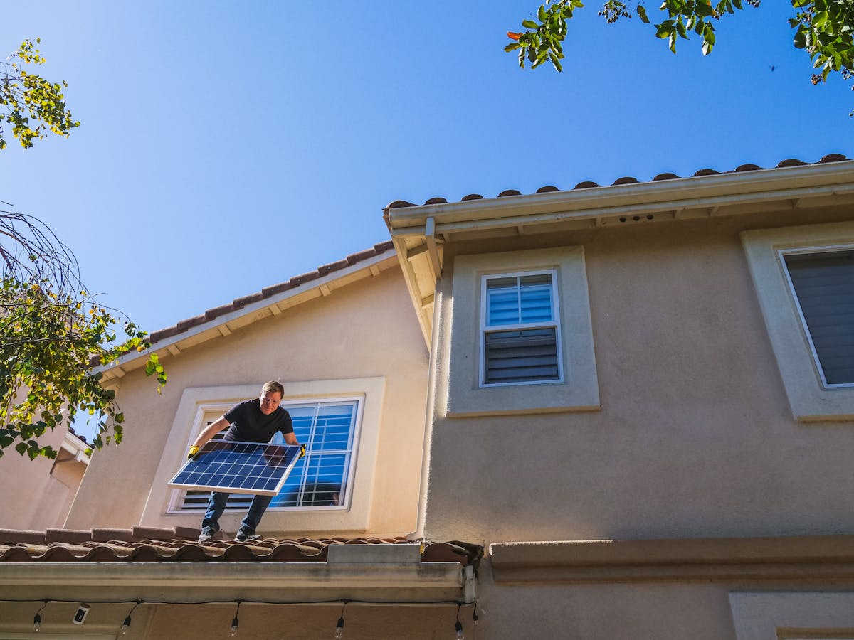
Grid‑Scale and Rooftop Implications
Higher module efficiency has cascading benefits for solar‑power deployment.
Benefits for Rooftop and Urban Installations
- More power per unit area—critical for limited roof space or facades.
- Lower balance‑of‑system (BoS) costs—fewer mounting structures, inverters, and cabling per installed watt.
- Improved aesthetics—tandems can be integrated into building‑integrated photovoltaics (BIPV) with custom colors and form factors.
Utility‑Scale and Grid Integration
On large solar farms, high‑efficiency tandems can:
- Reduce land usage or increase output on the same land area.
- Improve capacity factors when paired with advanced tracking systems.
- Enable hybrid configurations (e.g., agrivoltaics) where space is at a premium.
Analysts highlight that, if tandem modules reach mass‑production costs only modestly higher than silicon while offering 20–30% relative efficiency gains, the levelized cost of electricity (LCOE) from solar could drop significantly, further displacing fossil‑fuel generation.
Challenges: From Lab Breakthroughs to Terawatt Deployment
Despite remarkable progress, several hurdles must be overcome before perovskite–silicon tandems can achieve terawatt‑scale impact.
1. Long‑Term Reliability and Certification
Meeting or exceeding established standards (e.g., IEC 61215, IEC 61730) over decades of field exposure remains the biggest technical challenge. Prediction models must reconcile accelerated testing with real‑world degradation mechanisms.
2. Scalable, Reproducible Manufacturing
Transitioning from lab‑scale spin‑coated devices to gigawatt‑scale, high‑yield production requires:
- Uniform perovskite film deposition at high line speeds.
- Robust process windows tolerant to environmental and feedstock variations.
- Integration with existing silicon cell and module lines without overwhelming capital costs.
3. Supply Chains and Materials Sustainability
Although perovskites use relatively small amounts of raw material, scaling production demands reliable supply of high‑purity precursors, solvents, and specialty layers such as transparent conductive oxides.
4. Public Perception and Policy
Concerns over toxicity, newness of the technology, and long‑term stability must be addressed through transparent data, rigorous third‑party testing, and clear recycling and stewardship schemes. Policy incentives and standards will influence how quickly tandems are bankable in major markets.
Scientific Significance: A Frontier for Chemistry and Materials Science
Beyond commercial metrics, perovskite–silicon tandems are an exciting playground for fundamental science. Key research themes include:
- Defect physics in soft, ionic semiconductors.
- Ion migration and halide segregation under electric fields and illumination.
- Novel charge‑transport materials compatible with high‑band‑gap perovskites.
- Advanced characterization (e.g., time‑resolved photoluminescence, operando microscopy, synchrotron‑based techniques).
Interdisciplinary collaboration between synthetic chemists, thin‑film process engineers, device physicists, and reliability experts is essential. The field also provides valuable case studies in how rapidly a new material can move from academic curiosity to near‑commercial application when performance benefits are compelling.
Tools, Learning Resources, and Related Technologies
Researchers, students, and professionals interested in perovskite–silicon tandems can deepen their understanding using a mix of textbooks, online courses, and laboratory tools.
Recommended Reading and Courses
- Joule – Journal for high‑impact energy research.
- NREL Perovskite Solar Cells Overview for regularly updated status summaries.
- Massive open online courses (MOOCs) on photovoltaics and solar energy from platforms like Coursera and edX, often including perovskite modules.
Hands‑On Lab and Prototyping Tools
For university labs and R&D groups setting up perovskite research platforms, essential tools include:
- Gloveboxes with controlled atmosphere for air‑sensitive processing.
- Spin coaters or slot‑die coaters for thin‑film deposition.
- Solar simulators and quantum‑efficiency measurement systems.
Researchers and advanced hobbyists can also explore entry‑level lab hardware such as benchtop solar simulators and precision multimeters or source‑measure units. When purchasing measurement tools or reference solar modules from vendors (including marketplaces like Amazon), prioritize equipment with clear calibration standards and documented accuracy suitable for photovoltaic characterization.
Conclusion: Toward a Tandem‑Powered Energy Transition
Perovskite–silicon tandem solar cells exemplify how rapid advances in chemistry and materials science can reshape technological roadmaps. By combining the stability and industrial base of silicon with the tunability and high absorption of perovskites, tandems are on a trajectory to deliver module efficiencies once considered unattainable for mass‑market photovoltaics.
Key achievements over the last decade include:
- Surpassing 30% certified lab efficiencies.
- Substantially improving operational stability through compositional and interfacial engineering.
- Launching pilot manufacturing lines that integrate perovskite processing into silicon fabs.
Remaining challenges—in durability, large‑area manufacturing, lead stewardship, and public acceptance—are serious but tractable. If solved, tandem technology could become a cornerstone of a low‑carbon energy system, enabling more power from every rooftop and solar farm and helping accelerate decarbonization globally.
Additional Perspectives and Future Directions
Looking ahead, researchers are exploring:
- All‑perovskite tandems that stack two different perovskites without silicon, enabling ultra‑light, flexible modules.
- Perovskite tandems on thin‑film silicon, CIGS, or organic photovoltaics for specialized applications like aerospace or portable power.
- Integration with storage, such as pairing tandem PV with high‑energy‑density batteries and electrolyzers for green hydrogen production.
Computational materials design, machine learning‑guided process optimization, and high‑throughput experimentation are also becoming integral to discovering more stable compositions and scalable fabrication routes. For students and early‑career scientists, the field offers opportunities to contribute to both fundamental understanding and real‑world impact within a single research trajectory.
References / Sources
Selected reputable sources for further reading:
- National Renewable Energy Laboratory (NREL) – Perovskite Solar Cells:
https://www.nrel.gov/pv/perovskite-solar-cells.html - Helmholtz‑Zentrum Berlin – Perovskite Tandem Solar Cells:
https://www.helmholtz-berlin.de/projects/perovskite-tandem-solar-cells/index_en.html - Green, M. A., Dunlop, E. D., et al. “Solar cell efficiency tables (Version – continuously updated).” Progress in Photovoltaics: Research and Applications.
https://onlinelibrary.wiley.com/journal/1099159x - Editorial overview on tandem solar cells in Nature Energy:
https://www.nature.com/nenergy/ - International Energy Agency (IEA) – Solar Energy Technology Roadmap:
https://www.iea.org/reports/solar-pv
