
Perovskite Tandem Solar Cells: The Hottest Tech Pushing Solar Efficiency Beyond 30%
Perovskite and tandem solar cells have become the most watched materials‑science story in renewable energy. In just over a decade, perovskite solar cells have gone from scientific curiosity to lab devices exceeding 25% efficiency, while perovskite–silicon tandem cells have surged past 30% certified efficiency. This rapid progress is now translating into pilot production lines, major funding rounds, and intense interest across climate tech, semiconductor physics, and industrial engineering.
At the core of this trend is a simple idea with profound implications: stack two (or more) solar absorbers with different band gaps so that each portion of the solar spectrum is converted more efficiently than any single material could manage alone. Perovskites, with their tunable band gaps and low‑temperature processing, have emerged as the ideal partner for incumbent crystalline silicon.
Below, we explore how these solar cells work, why efficiency records keep falling, the remaining obstacles around stability and lead, and what it will take to see tandem modules on rooftops, deserts, and even in space.
Mission Overview: Why Perovskite and Tandem Solar Cells Matter
The “mission” of perovskite and tandem solar cells is straightforward but ambitious: reduce the cost of solar electricity by increasing efficiency without drastically increasing manufacturing costs or environmental impact. In energy‑system terms, even a few percentage points of efficiency gain in modules can cascade through the entire value chain, lowering balance‑of‑system (BOS) costs, soft costs, and land requirements.
Traditional crystalline silicon solar cells are extremely mature, with gigawatt‑scale factories around the world. However, single‑junction silicon cells are fundamentally constrained by the Shockley–Queisser limit, which caps theoretical efficiency near 33% under standard illumination, with practical commercial devices clustering in the mid‑20% range.
Tandem architectures directly target this ceiling. By stacking a wide‑band‑gap perovskite top cell over a lower‑band‑gap silicon bottom cell, the tandem captures more of the solar spectrum with less thermalization loss:
- High‑energy blue and green photons are absorbed by the perovskite layer.
- Lower‑energy red and near‑infrared photons pass through to the silicon, which converts them efficiently.
- The overall voltage and current are engineered either in series (2‑terminal) or independently (4‑terminal) for maximal power output.
“Tandem architectures allow us to push well beyond the traditional limits of silicon photovoltaics without discarding the enormous manufacturing base already in place.” — Adapted from research perspectives at the U.S. National Renewable Energy Laboratory (NREL)
Background: From Silicon Dominance to Perovskite Disruption
For decades, crystalline silicon has dominated the photovoltaic (PV) market, currently providing roughly 90–95% of deployed solar capacity worldwide. Its advantages are clear: abundant raw materials, established supply chains, and ever‑falling costs driven by economies of scale and incremental process improvements like PERC, TOPCon, and heterojunction technologies.
Around 2012–2013, a new class of materials burst onto the scene: metal halide perovskites. Defined by the ABX3 crystal structure (where A is a monovalent cation like methylammonium (MA), formamidinium (FA), or cesium (Cs); B is typically lead (Pb) or tin (Sn); and X is a halide such as iodide (I), bromide (Br), or chloride (Cl)), these compounds showed astonishing photovoltaic performance even in early prototypes.
Key properties that made perovskites disruptive include:
- Tunable band gap: By mixing halides and cations, researchers can continuously tune the band gap between ~1.2 and ~2.3 eV, enabling perfect pairing with silicon (~1.1 eV) in tandems.
- Strong light absorption: Perovskites absorb sunlight strongly, allowing active layers only a few hundred nanometers thick.
- Solution processability: They can be deposited via low‑temperature solution processes (spin‑coating, slot‑die coating, inkjet printing) or vapor deposition, opening pathways to cheaper, scalable manufacturing.
- Defect tolerance: The perovskite structure can tolerate a relatively high density of defects while maintaining good electronic properties, unlike many traditional semiconductors.
As a result, perovskite single‑junction cells raced from ~3% efficiency in early demonstrations to over 25% in just over a decade, a speed of improvement unmatched in PV history.
Technology: How Perovskite and Tandem Solar Cells Work
At their core, perovskite solar cells follow the same basic principles as all photovoltaic devices: photons create electron–hole pairs, which are separated and collected by built‑in electric fields at junctions or interfaces, generating current and voltage. What distinguishes perovskites is how easily their optoelectronic properties can be engineered.
Perovskite Single‑Junction Cell Architecture
A typical high‑efficiency perovskite solar cell includes:
- Substrate: Often glass with a transparent conductive oxide (TCO) like indium tin oxide (ITO) or fluorine‑doped tin oxide (FTO).
- Electron transport layer (ETL): Materials such as TiO2, SnO2, or organic small molecules that selectively collect electrons.
- Perovskite absorber layer: A mixed‑cation, mixed‑halide perovskite tuned for a ~1.5–1.7 eV band gap.
- Hole transport layer (HTL): Organic (e.g., Spiro‑OMeTAD) or inorganic (e.g., NiOx) materials that collect holes.
- Back contact: Typically gold, silver, or conductive carbon layers.
Variants such as n–i–p and p–i–n structures rearrange these layers to optimize charge extraction, stability, and compatibility with tandem integration.
Silicon–Perovskite Tandem Architectures
Tandem solar cells stack a perovskite cell on top of a silicon cell. Two main architectures dominate:
- 2‑terminal (monolithic) tandems: The perovskite and silicon sub‑cells are electrically connected in series with a shared current. The top perovskite typically has a band gap ~1.7–1.8 eV, optimized to balance current with the silicon bottom cell. This architecture is most compatible with current silicon module production lines.
- 4‑terminal (mechanically stacked) tandems: The perovskite and silicon cells operate independently, each at its own maximum power point, with separate contacts. This configuration offers flexibility and higher theoretical efficiency but is more complex at the module/system level.
Benefits of tandem designs include:
- Reduced thermalization losses for high‑energy photons.
- Better utilization of near‑infrared light by the silicon bottom cell.
- Higher open‑circuit voltage (VOC) and potentially better performance under high‑irradiance or high‑temperature conditions.
As of late 2025, multiple research groups and companies have reported perovskite–silicon tandem efficiencies above 30%, with laboratory champions approaching 34% in closely controlled conditions, according to efficiency tables curated by institutions such as NREL and academic consortia.
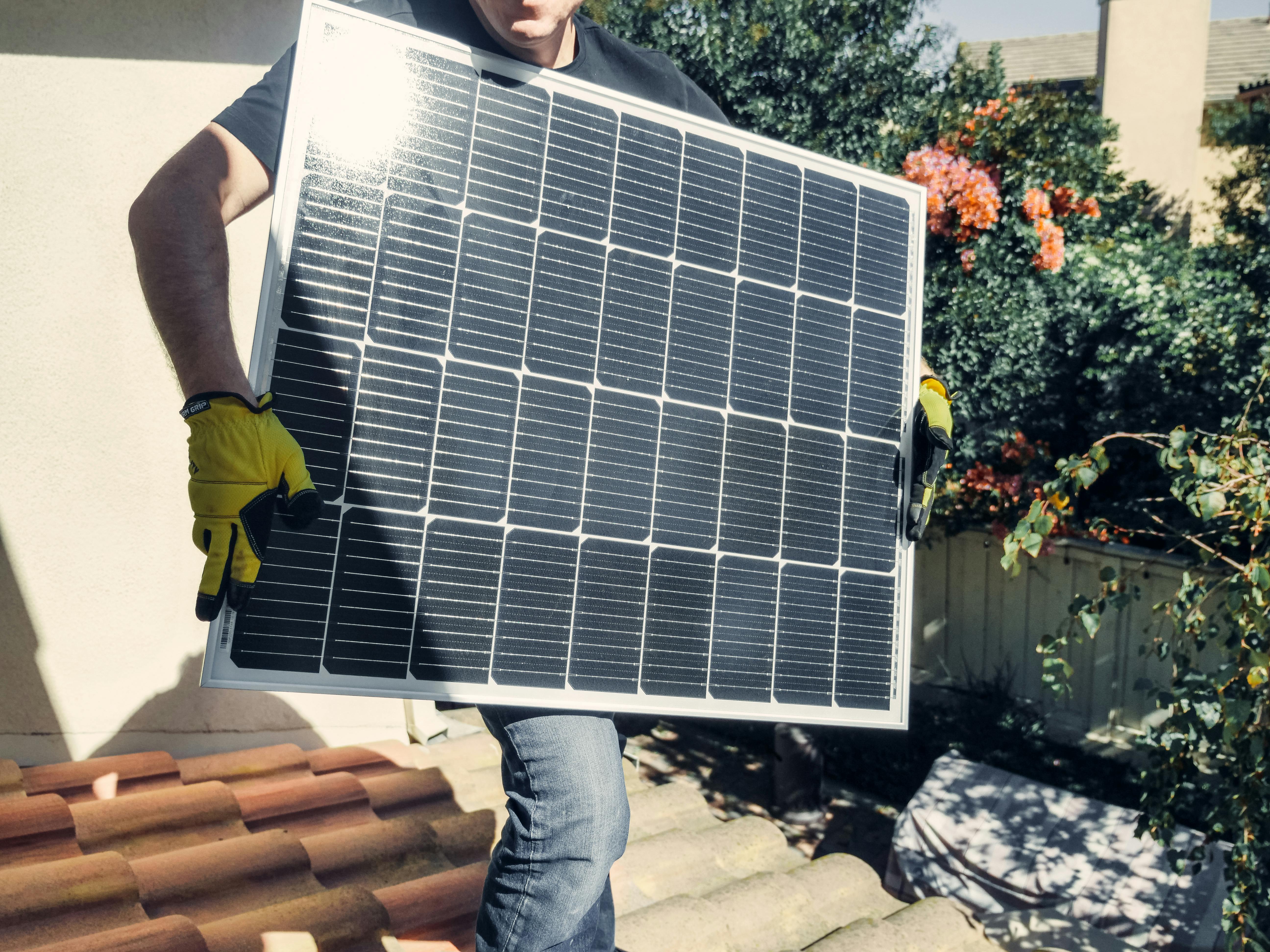
Visualizing Perovskite and Tandem Solar Technology

Scientific Significance: Pushing the Shockley–Queisser Limit
In single‑junction solar cells, the Shockley–Queisser (S–Q) limit arises because photons with energy below the band gap are not absorbed, while those with energy well above the band gap lose their excess energy as heat. The optimum band gap under the standard AM1.5G spectrum is around 1.3–1.4 eV, which is close to silicon’s 1.1 eV but not perfect.
Tandem cells break through this limit by effectively approximating a multi‑step energy staircase for photons:
- The perovskite top cell, with a wider band gap, captures high‑energy photons and converts them to electricity at a higher voltage.
- Lower‑energy photons transmit to the silicon cell, which operates near its optimal band gap for current generation.
- The combined device reduces both transmission and thermalization losses compared with a single absorber.
Theoretically, a well‑designed 2‑junction tandem can achieve efficiencies in the mid‑40% range under concentrated sunlight and high 30% range under standard conditions. When realized in cost‑effective modules, this performance offers:
- Lower levelized cost of electricity (LCOE) due to higher energy yield per unit area.
- Reduced land and mounting structure requirements.
- Improved economics for space‑constrained applications (rooftops, urban infrastructure, vehicles).
“Perovskite–silicon tandems exemplify how fundamental semiconductor physics can directly reshape the economics of decarbonization.” — Paraphrased from editorials in Joule and related journals
Major Milestones and Commercialization Moves
The trajectory of perovskite and tandem solar technology is marked by dramatic efficiency gains and increasing commercial engagement. While specific record numbers shift as new results appear, the broad trend is clear: perovskite–silicon tandems surpassed 30% certified efficiency in the early 2020s and have continued to inch upward with improved interface engineering and light‑management strategies.
Key Technical Milestones
- Single‑junction perovskite cells exceeding 25% in lab settings.
- Monolithic tandem cells above 30% certified efficiency, verified by independent test labs.
- Demonstrations of operational stability approaching or surpassing several thousand hours under accelerated stress tests.
- Prototype modules (tens to hundreds of watts) produced using scalable coating methods such as slot‑die coating and vapor deposition.
Industrial and Investment Milestones
Over the last few years, energy‑tech media have highlighted:
- Joint development agreements between perovskite startups and established silicon PV manufacturers.
- Pilot production lines in Europe, Asia, and North America focused on tandem modules compatible with existing infrastructure.
- Significant venture capital and strategic corporate investment into perovskite materials, encapsulation technologies, and tandem module integration.
Articles and explainer videos often emphasize LCOE comparisons, showing that a modest 3–5 percentage‑point boost in module efficiency can substantially reduce system‑level costs, especially in high labor‑cost regions where installation dominates expenses.
Manufacturing Methodologies and Device Engineering
Scaling perovskite and tandem cells from lab to factory demands robust, repeatable processes compatible with high throughput and low defect rates. Current research and industrial development focus on several core methodologies.
Deposition Techniques
- Spin‑coating: Widely used in research for its simplicity and uniformity on small areas, but less suitable for roll‑to‑roll mass production.
- Slot‑die coating: A scalable technique where liquid precursor inks are dispensed through a narrow slot onto moving substrates, enabling continuous processing.
- Blade coating and bar coating: Mechanical spreading methods that can be tuned for film thickness and uniformity over large areas.
- Thermal evaporation and hybrid vapor–solution processes: Offer more precise control over composition and thickness, potentially improving reproducibility and film quality.
Compositional and Interface Engineering
To improve both efficiency and stability, materials scientists employ:
- Mixed cations (FA/MA/Cs): Combining organic and inorganic cations to optimize tolerance factors and suppress phase instabilities.
- Mixed halides (I/Br/Cl): Tuning band gaps for tandem optimization while managing halide segregation under illumination.
- Passivation layers: Ultra‑thin interlayers or molecular treatments that reduce surface and grain‑boundary recombination sites.
- Advanced charge‑transport layers: Inorganic ETLs/HTLs (SnO2, NiOx, CuSCN) that combine good band alignment with better thermal and chemical stability than many organic counterparts.
Interface and band‑alignment engineering are particularly critical in tandem devices, where any losses at the perovskite/silicon junction can easily negate the theoretical gains from stacking absorbers.
Challenges: Stability, Lead Toxicity, and Scaling
Despite rapid progress, key challenges still separate laboratory prototypes from bankable commercial products. Three issues dominate the conversation across scientific, industrial, and policy communities: stability, lead toxicity, and manufacturability at scale.
Stability and Degradation
Metal halide perovskites are inherently sensitive to environmental stressors:
- Moisture and oxygen can induce phase changes and decomposition.
- Heat accelerates diffusion and chemical reactions at interfaces.
- UV light can damage certain transport layers and trigger perovskite degradation.
Current mitigation strategies include:
- Compositional engineering: Using FA/Cs mixes, reduced MA content, and carefully balanced halides.
- Robust encapsulation: Multilayer barrier films, glass–glass laminates, and edge‑sealing materials tailored for perovskite chemistry.
- Interface protection: UV‑stable transport layers, interlayers that block ion migration, and diffusion barriers.
- Reliability testing: Accelerated stress tests (damp heat, thermal cycling, light soaking) following or extending IEC PV standards.
Lead Toxicity
Most high‑performance perovskite formulations currently contain lead, prompting environmental and regulatory concerns. While the amount of lead per watt of PV is small compared with many existing technologies, public acceptance depends on minimizing leakage risks over the entire life cycle.
Research directions include:
- Lead‑reduced and lead‑free perovskites: Tin‑based and mixed‑metal perovskites, though these often suffer from instability and lower efficiency.
- Encapsulation and containment: Ensuring that even in breakage or fire, lead is not easily released into the environment.
- Recycling and end‑of‑life strategies: Designing modules for disassembly and material recovery, including closed‑loop perovskite ink reuse.
Scalability and Manufacturing Integration
Moving from 1 cm² lab cells to full‑size modules (over 1 m²) is non‑trivial. Issues such as film uniformity, pinholes, defect density, and interconnection yield dominate at scale. Additionally, tandems must integrate seamlessly with well‑optimized silicon production lines:
- Matching thermal budgets so that high‑temperature silicon steps do not damage perovskite layers.
- Maintaining throughput and yield comparable to state‑of‑the‑art silicon lines.
- Qualifying new materials and processes through bankability‑oriented testing regimes demanded by financiers and insurers.
“The transition from record cells to reliable modules is where new PV technologies most often stumble.” — Summarized from perspectives in Nature Energy
Emerging Applications and Use Cases
As perovskite and tandem technologies mature, several application domains stand out where higher efficiency and unique form factors provide significant advantages.
- Residential and commercial rooftops: Space is limited and labor is expensive, so higher‑efficiency modules can meaningfully reduce total system cost and simplify achieving net‑zero energy targets.
- Building‑integrated photovoltaics (BIPV): Perovskites’ tunable colors and potential for semi‑transparent devices make them attractive for solar windows and façade elements.
- Portable and off‑grid power: Lightweight, flexible perovskite modules can be integrated into backpacks, tents, and emergency systems where mass and transportability matter.
- Vehicle‑integrated photovoltaics (VIPV): Electric vehicles and trucks can host thin‑film or tandem modules on roofs and body panels to extend range under sunlight.
- Space applications: High‑specific‑power (W/kg) perovskite and tandem devices are being explored for satellites and high‑altitude platforms, potentially reducing launch costs relative to traditional space‑grade III–V cells.
Tools and Resources for Researchers and Enthusiasts
For students, engineers, and policymakers wanting to understand or work with perovskite and tandem PV, a growing ecosystem of tools and resources is available.
Technical Literature and Databases
- Peer‑reviewed journals such as Joule, ACS Energy Letters, Energy & Environmental Science, and Advanced Energy Materials regularly publish cutting‑edge perovskite and tandem research.
- Public efficiency tables and charts from institutions like NREL provide updated benchmarks for different PV technologies.
- Preprint servers like arXiv (materials science) host early‑stage results and modeling studies.
Educational Content and Videos
- YouTube channels focused on renewable energy and materials science, such as detailed explainers on tandem PV physics and manufacturing tours of pilot perovskite lines.
- University lecture series and MOOCs on semiconductor devices and photovoltaic engineering, which often include updated modules on perovskites.
- Professional talks and webinars on platforms like LinkedIn and conference channels that discuss bankability and policy aspects of new PV technologies.
Hands‑On Learning Aids
While fully fledged perovskite fabrication is not yet accessible to hobbyists, those interested in solar fundamentals can learn with educational kits and measurement tools. For example, portable solar irradiance meters and module testers allow users to explore how orientation, shading, and temperature affect performance.
Trends in Media, Finance, and Policy
Perovskite and tandem solar cells consistently attract attention on social media platforms, energy‑tech news outlets, and investment channels. Several factors contribute to this sustained interest.
- Visual appeal: Colorful thin films, flexible cells, and roll‑to‑roll demos make for compelling video content on YouTube, TikTok, and other platforms.
- Record‑setting headlines: Every new efficiency milestone or extended stability demo generates spikes in Google Trends and specialist newsletters.
- Climate narratives: Tandem PV is frequently framed as a key enabling technology for accelerated decarbonization, bridging the gap between current renewable deployment and ambitious net‑zero targets.
- Investment and policy implications: Venture capital announcements, government R&D programs, and clean‑energy industrial policies often highlight support for advanced PV technologies, including perovskites.
Future Outlook: From Pilot Lines to Terawatt Scale
Looking toward the late 2020s and early 2030s, the central question is not whether perovskite and tandem cells can be efficient—that has already been demonstrated—but whether they can be produced and deployed at terawatt scale with sufficient durability and safety.
Key milestones to watch include:
- Bankable 25–30 year warranties: Once manufacturers can confidently guarantee tandem modules for lifetimes comparable to today’s silicon panels, mainstream adoption can accelerate.
- Standardized reliability protocols: Industry‑wide testing standards tailored to perovskite chemistry will help financiers compare products and reduce perceived risk.
- Integration into utility‑scale projects: Demonstration plants that operate for multiple years with high uptime and predictable degradation will provide real‑world data.
- Recycling and circularity frameworks: Well‑defined end‑of‑life strategies will address environmental concerns, particularly around lead‑containing devices.
Many experts anticipate a hybrid future in which classic silicon remains the “workhorse” absorber, while perovskite layers act as efficiency boosters in tandem or multi‑junction configurations. Over time, fully perovskite‑based tandems and perovskite–III–V combinations may find niches in high‑performance or space‑constrained markets.
Conclusion: A Rare Convergence of Physics, Materials, and Climate Impact
Perovskite and tandem solar cells represent a rare case where fundamental advances in solid‑state physics and chemistry are swiftly migrating into technologies with enormous practical impact. By surpassing the efficiency limits of single‑junction silicon while leveraging existing manufacturing infrastructure, perovskite–silicon tandems offer a realistic path to cheaper, more compact, and more versatile solar energy systems.
Success is not guaranteed: stability, toxicity management, and scaling remain formidable challenges. However, the pace of progress—from single‑digit perovskite efficiencies to >30% tandem devices in roughly a decade—suggests that this field will remain at the forefront of energy‑tech innovation for years to come.
For scientists, engineers, investors, and policymakers, the message is clear: tracking perovskite and tandem solar developments is no longer optional. These technologies are rapidly moving from “promising” to “inevitable” in the broader story of global decarbonization.
Additional Insights: How Readers Can Stay Informed and Engaged
To draw the most value from ongoing developments in perovskite and tandem solar technology, consider the following practical steps:
- Follow key research groups and institutions: Many leading labs maintain active websites and social media accounts where they share new results, open‑access preprints, and explanatory threads aimed at non‑specialists.
- Subscribe to specialized newsletters: Clean‑energy and materials‑science newsletters often provide curated round‑ups of the most important perovskite and tandem advances without requiring deep technical expertise.
- Engage with policy and standards discussions: Public consultations on renewable‑energy policies, building codes, and recycling regulations increasingly touch on advanced PV technologies; informed feedback can help shape responsible deployment pathways.
- Support transparent pilot projects: Utilities, universities, and companies that openly share performance data from perovskite and tandem pilots accelerate collective learning and derisk adoption for everyone.
Keeping an eye on these channels will help you distinguish between genuine breakthroughs, incremental improvements, and over‑hyped announcements, allowing more informed decisions in research, investment, and policy contexts.
References / Sources
Selected reputable sources for deeper reading:
- National Renewable Energy Laboratory (NREL) — Best Research-Cell Efficiency Chart: https://www.nrel.gov/pv/cell-efficiency.html
- Review on metal halide perovskite solar cells in Nature Energy: https://www.nature.com/subjects/perovskite-solar-cells
- Perovskite solar cell research highlights at the U.S. Department of Energy: https://www.energy.gov/eere/solar/perovskite-solar-cells
- Journal Joule — Advanced PV and tandem solar research articles: https://www.cell.com/joule/home
- General PV fundamentals from the Fraunhofer Institute for Solar Energy Systems (ISE): https://www.ise.fraunhofer.de/en/key-topics/photovoltaics.html
