
Why Perovskite–Silicon Tandem Solar Cells Could Rewrite the Future of Solar Power
In this article, we unpack the crystal chemistry behind perovskites, how tandem architectures break through the efficiency ceiling of silicon, the hard problems of stability and lead safety, and what the latest pilot lines and field tests reveal about when this technology might hit rooftops and utility-scale solar farms.
Perovskite–silicon tandem solar cells sit at the intersection of chemistry, materials science, and renewable-energy engineering. By stacking a perovskite absorber on top of a conventional crystalline-silicon cell, researchers are now reporting certified power conversion efficiencies above 33%, edging close to the theoretical limits of multi-junction photovoltaics. Behind those headlines lies a dense web of crystal engineering, interface chemistry, degradation pathways, and emerging manufacturing know‑how that will determine whether tandems become the next dominant photovoltaic (PV) technology.
At the heart of this revolution are hybrid organic–inorganic lead halide perovskites, typically described by the formula ABX3, where A is a monovalent cation (such as methylammonium, formamidinium, or cesium), B is Pb2+ (lead), and X is a halide (I−, Br−, Cl−). Their unique combination of strong light absorption, long carrier diffusion lengths, defect tolerance, and solution-processability has allowed performance to climb from around 3% in 2009 to over 26% for single-junction perovskite cells and beyond 33% for tandems by the mid‑2020s.

Mission Overview: Why Perovskite–Silicon Tandems Matter
Conventional single-junction silicon solar cells are approaching their practical efficiency ceiling of about 26–27%, constrained by fundamental thermodynamic limits (the Shockley–Queisser limit) and real‑world material losses. Tandem architectures aim to break this ceiling by stacking materials with different band gaps, each harvesting a distinct slice of the solar spectrum.
In a typical perovskite–silicon tandem:
- The top perovskite cell has a wider band gap (~1.7–1.8 eV), optimized to absorb high-energy visible photons.
- The bottom silicon cell, with a band gap of ~1.12 eV, efficiently captures lower-energy red and near‑infrared photons transmitted through the perovskite layer.
This spectral splitting allows tandems to convert more of the incident solar energy into electricity than either material alone, lifting theoretical efficiencies beyond 30%. As of 2025–2026, several research groups and industrial consortia report certified tandem efficiencies in the 31–34% range, often using industrially relevant wafer sizes.
“Tandem perovskite–silicon architectures give us a credible pathway toward module efficiencies in the mid‑30% range while still leveraging the massive silicon manufacturing ecosystem.”
— Adapted from commentary by Prof. Michael Grätzel (EPFL) and colleagues in recent tandem PV reviews.
Background: The Chemistry of Perovskite Absorbers
The label “perovskite” describes a crystal structure rather than a single compound. In photovoltaics, the most relevant family is the hybrid organic–inorganic lead halide perovskites with the ABX3 structure. The chemistry of each site critically tunes stability, band gap, and defect physics.
A‑Site: Organic and Inorganic Cations
The A‑site cation occupies the cuboctahedral void in the perovskite lattice and has a disproportionate influence on phase stability and tolerance to temperature and humidity.
- Methylammonium (MA+): Enabled early efficiency breakthroughs but is relatively volatile and thermally unstable.
- Formamidinium (FA+): Provides a near‑optimal band gap (~1.48 eV for FAPbI3) but tends to form non‑perovskite phases unless stabilized by mixed cations or halides.
- Cesium (Cs+): An inorganic cation that improves thermal and structural stability when partially substituted into FA/MA perovskites.
Modern “triple‑cation” perovskites often blend FA, MA, and Cs to balance efficiency and robustness, especially under operational stress.
X‑Site: Halide Tuning for Band Gap Control
Halide composition controls the band gap, which is crucial for tandem design:
- Iodide‑rich (e.g., FAPbI3): Narrower band gaps (~1.48 eV), good for single‑junction cells or bottom cells in all‑perovskite tandems.
- Mixed iodide–bromide (I/Br): Tailored to ~1.7–1.8 eV for the top cell in Si tandems.
- Higher bromide fractions: Widen the band gap further but raise susceptibility to phase segregation under illumination.
Chemists now routinely “band-gap engineer” perovskites through precise halide ratios combined with additives that suppress segregation and defect formation.
B‑Site and Emerging Lead‑Free Systems
Most commercial‑grade perovskite devices still rely on Pb2+ because it yields the best combination of electronic quality and defect tolerance. However, environmental and regulatory concerns drive active research into:
- Sn‑based perovskites (e.g., FASnI3), which avoid lead but suffer from rapid Sn2+ oxidation and high defect densities.
- Mixed Pb–Sn alloys, which can tune band gap while partially reducing Pb content.
- Double perovskites and related structures (e.g., Cs2AgBiBr6), promising for toxicity reduction but still far behind in efficiency.

Technology: How Perovskite–Silicon Tandem Solar Cells Work
Perovskite–silicon tandems are generally fabricated in two architectures: monolithic two‑terminal (2T) devices and mechanically stacked four‑terminal (4T) devices.
Monolithic (2T) Tandems
In a monolithic tandem, the perovskite and silicon sub‑cells are connected in series and share a common current path. The device is deposited directly on a textured silicon wafer or on top of an interlayer stack. Key elements include:
- Front contact (e.g., transparent conductive oxide such as ITO or IZO).
- Electron-transport layer (ETL) (e.g., SnO2, TiO2 derivatives).
- Perovskite absorber with tuned band gap (~1.7–1.8 eV).
- Hole-transport layer (HTL) (e.g., Spiro‑OMeTAD derivatives, PTAA, or doped polymers).
- Recombination layer / tunnel junction that electrically connects the perovskite and silicon sub‑cells.
- Silicon heterojunction or PERC/PERT cell serving as the bottom absorber.
- Rear contact and encapsulation.
Because the sub‑cells are in series, device performance is limited by current matching: both perovskite and silicon layers must generate similar photocurrents to avoid “bottlenecking” the tandem’s output. This constraint makes optical and thickness optimization critical.
Four‑Terminal (4T) Tandems
In 4T tandems, the perovskite and silicon cells operate independently with separate electrical contacts. Light first passes through a semi‑transparent top perovskite cell, and transmitted light is harvested by a separate silicon module.
4T designs:
- Relax current‑matching constraints.
- Offer flexibility in independently replacing or upgrading the top or bottom cell.
- Introduce added optical and mechanical complexity and potentially higher cost.
Deposition and Manufacturing Strategies
Scalability is a major focus of industrial R&D. Approaches under active development include:
- Solution coating (slot‑die, blade coating, inkjet printing) for low‑cost, roll‑to‑roll compatible processing.
- Vacuum deposition (co‑evaporation, hybrid solution/evaporation) for uniform large‑area films and precise composition control.
- Hybrid routes, such as vapor‑assisted solution processing and gas‑quenching techniques, to improve crystal quality at scale.
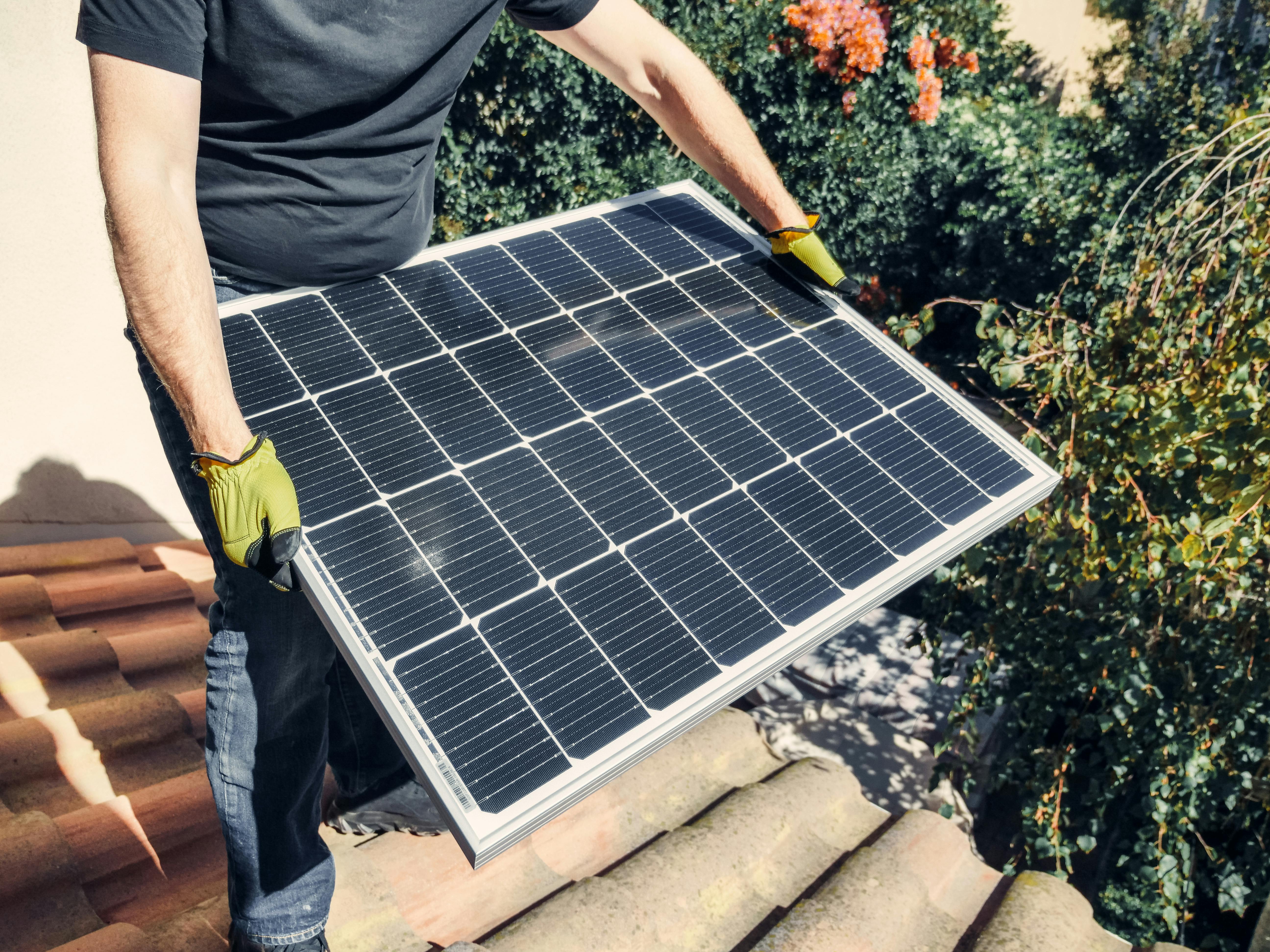
Commercial pilot lines from companies such as Oxford PV, Saule Technologies, and several Chinese manufacturers have demonstrated square‑meter‑scale tandem and perovskite modules undergoing IEC reliability testing.
Scientific Significance: Why the Chemistry Matters
The perovskite–silicon tandem story is fundamentally a chemistry story. Incremental efficiency gains often track specific advances in crystal design, interface chemistry, or defect passivation.
Defect Tolerance and Passivation
Unlike many semiconductors, lead halide perovskites show remarkable “defect tolerance”: certain point defects create shallow energy levels that minimally affect carrier lifetimes. Nonetheless, non‑radiative recombination at grain boundaries and interfaces still limits performance.
- Lewis base additives (e.g., thiocyanates, pyridinium salts) can coordinate under‑coordinated Pb2+ sites.
- Alkali halides and quasi‑2D surface layers help “heal” surface traps.
- Self‑assembled monolayers (SAMs) at the perovskite/transport‑layer interface finely tune band alignment and reduce recombination.
Interface Chemistry in Tandems
Interfaces between perovskite, transport layers, and silicon sub‑cells are hotspots of chemical reactivity and performance losses. Degradation can be triggered by:
- Interdiffusion of mobile ions (e.g., I−, MA+).
- Chemical reactions with metal electrodes (e.g., Ag, Cu) leading to halide migration.
- Acidic dopants in organic HTLs attacking adjacent layers.
Careful selection of inorganic transport layers (e.g., NiOx, SnO2) and barrier layers, combined with chemically compatible dopants, is now central to all high‑stability tandem designs.
“Most of our recent efficiency gains no longer come from the perovskite bulk alone, but from the dozen or so nanometer‑scale interfaces where chemistry quietly determines whether carriers make it to the contacts or die along the way.”
— Paraphrased from recent comments by Prof. Nam‑Gyu Park, Sungkyunkwan University.
Milestones: Efficiency and Commercialization Updates
Perovskite and tandem PV have experienced one of the steepest efficiency learning curves in the history of photovoltaics. According to regularly updated charts from the National Renewable Energy Laboratory (NREL), certified efficiencies have progressed rapidly.
Key Efficiency Milestones
- 2009–2012: Early perovskite solar cells with efficiencies <10% and short lifetimes.
- 2015–2018: Single‑junction perovskites surpass 20%; the first silicon tandems exceed 23–25%.
- 2019–2022: Tandems reach and pass 29–30%; stability tests hit the 1,000–2,000 hour mark at elevated temperatures and light intensity.
- 2023–2025: Multiple lab‑scale tandems report certified efficiencies of ~31–34% using industrial silicon architectures and larger cell areas.
By 2025–2026, several industrial players report:
- Pilot‑scale tandem modules undergoing IEC 61215 / 61730 testing.
- Accelerated aging equivalent to 20–25 years under standard operating conditions.
- Prototype rooftop and building‑integrated PV (BIPV) demonstrators using perovskite top cells.
Commercialization Announcements
Announcements from companies such as Oxford PV and others highlight:
- Commissioning of tandem cell production lines in Europe and Asia.
- Partnerships with established glass and module manufacturers.
- Certification campaigns aimed at bankability for utility‑scale deployment.
Stability and Degradation: The Achilles’ Heel
While efficiency headlines dominate, long‑term stability under real‑world conditions is still the key question for widespread deployment. Historically, perovskite films have been vulnerable to a range of degradation mechanisms.
Major Degradation Pathways
- Moisture ingress: Water can trigger phase transitions and hydrolysis of organic cations, leading to a yellow, non‑perovskite phase.
- Thermal stress: Elevated temperatures encourage ion migration, phase segregation (particularly in I/Br mixtures), and out‑diffusion of volatile components.
- UV and photo‑oxidation: UV light and oxygen together can drive the formation of Pb0 and decomposition of organic components.
- Electric field–driven ion migration: Halide and cation motion under bias causes hysteresis and long‑term performance drift.
Stabilization and Encapsulation Strategies
Recent progress combines materials design with robust encapsulation:
- 2D/3D perovskite interfaces that form a protective, more hydrophobic outer layer.
- Cross‑linkable organic spacers in quasi‑2D structures to reduce ion mobility.
- Inorganic transport layers less prone to chemical reactions than doped organics.
- Advanced encapsulants and edge seals similar to those used in OLED and high‑end silicon modules, blocking water and oxygen.
Industrial groups now routinely report perovskite and tandem modules passing thousands of hours of damp‑heat and thermal‑cycling tests, though matching the multi‑decade record of crystalline silicon remains a work in progress.
Lead vs. Lead‑Free: Environmental and Regulatory Considerations
The outstanding device performance of lead‑based perovskites has prompted serious discussions about environmental responsibility. The amount of lead per square meter is relatively small compared with some legacy batteries, but uncontrolled release during manufacturing, operation, or end‑of‑life is unacceptable.
Risk Mitigation Strategies for Lead‑Based Perovskites
- Robust encapsulation to prevent leaching in the event of module damage.
- Lead‑absorbing interlayers that immobilize Pb2+ in case of perovskite breakdown.
- Recycling protocols that recover and safely process lead at end‑of‑life, similar to existing electronic‑waste streams.
Regulators in the EU, US, and Asia are actively examining how to classify and govern perovskite modules, with many experts arguing that strict encapsulation and recycling standards can adequately manage risk, especially compared with the environmental damage avoided by decarbonizing power generation.
Progress and Limits of Lead‑Free Alternatives
Tin‑based and other lead‑free systems are a vital research direction but currently lag in both efficiency and stability. As of mid‑2020s, state‑of‑the‑art Sn‑based perovskite cells trail their Pb‑based counterparts by several percentage points and show faster degradation under ambient conditions. For tandem commercialization in the 2020s, lead‑containing perovskites with stringent encapsulation and recycling are likely to dominate.
Applications and Impact on the Energy Transition
Perovskite–silicon tandems dovetail with the urgent need to decarbonize power systems. Higher conversion efficiencies can reduce the levelized cost of electricity (LCOE) by cutting balance‑of‑system expenses and land requirements per watt installed.
High‑Value Deployment Scenarios
- Rooftop and urban environments, where space is limited and each square meter must deliver maximum wattage.
- Building‑integrated PV (BIPV), where semi‑transparent and color‑tunable perovskite top cells offer new design freedom.
- Industrial and commercial sites, where lower LCOE and higher energy density can accelerate payback times.
- Potential space applications, leveraging lightweight, high‑efficiency perovskite layers atop silicon or flexible substrates.
In system‑level modeling, upgrading from 22–23% silicon modules to 30%‑plus tandems can reduce required install area and balance‑of‑system cost by 10–20%, depending on location and design assumptions.

Tools, Learning Resources, and Related Technologies
Researchers and engineers working on perovskite–silicon tandems rely on a mix of experimental, computational, and characterization tools.
Laboratory and Educational Resources
- For hands‑on solar cell education, devices such as the Eisco Solar Cell Educational Kit can help students grasp basic IV curves, shading effects, and module behavior.
- Researchers often supplement laboratory work with high‑throughput computation and machine learning to explore vast compositional spaces, as reviewed in recent articles in journals like Joule and Energy & Environmental Science.
Further Reading and Media
- Regular efficiency and technology updates from the NREL Best Research-Cell Efficiency Chart.
- Perspective and explainer articles on tandem solar cells in Nature Energy collections on perovskite photovoltaics.
- Conference talks on YouTube from meetings such as the IEEE PVSC and the Materials Research Society (MRS), where leading groups share their latest tandem results.
- Professional commentary on LinkedIn from PV experts and companies like Oxford PV and others, discussing manufacturing scale‑up and bankability.
Challenges Ahead: From Pilot Lines to Terawatts
Despite impressive laboratory and pilot‑scale achievements, multiple obstacles remain before perovskite–silicon tandems can deliver terawatt‑scale impact.
Key Technical and Commercial Challenges
- Long‑Term Stability: Demonstrating 25+ year lifetimes across varied climates, including desert, tropical, and cold environments.
- Manufacturing Yield: Achieving high‑throughput, low‑defect deposition of perovskite layers across large areas and textured silicon surfaces.
- Cost and Supply Chains: Ensuring that precursors, encapsulants, and production equipment remain cost‑competitive and scalable.
- Standards and Certification: Updating PV testing standards to adequately capture new degradation modes specific to perovskites and tandems.
- Public Perception and Regulation: Addressing concerns about lead content through transparent safety data, strict regulations, and demonstrated recycling practices.
“The step from a world‑record cell in a glovebox to a gigawatt of installed capacity on rooftops is massive. It demands not only good physics and chemistry, but also robust engineering, manufacturing, and policy frameworks.”
— Synthesized from remarks by multiple speakers at recent PV and materials conferences.
Conclusion: A Chemistry‑Driven Path to Next‑Gen Solar
Perovskite–silicon tandem solar cells exemplify how modern chemistry, materials science, and device engineering can converge to push a mature technology into a new performance regime. By exploiting complementary band gaps, finely tuned halide compositions, and meticulously engineered interfaces, tandems are already surpassing 33% efficiency in the laboratory and showing promising stability in pilot modules.
The coming decade will test whether these advances can be translated into reliable, bankable products that operate for decades in harsh environments. Success will depend not only on further gains in efficiency and stability, but also on responsible management of lead, robust recycling programs, and thoughtful integration into existing energy systems. If those hurdles are cleared, perovskite–silicon tandems could play a central role in accelerating the global clean‑energy transition and making high‑efficiency solar the default choice for rooftops, industries, and large‑scale power plants.
Additional Insights: How to Stay Current in a Fast‑Moving Field
The pace of progress in perovskite and tandem photovoltaics is unusually rapid. For students, practitioners, or investors wanting to stay informed, the following practices can be valuable:
- Track preprints on arXiv (applied physics) and ChemRxiv for early results.
- Follow major PV and materials journals (e.g., Joule, Advanced Energy Materials, Energy & Environmental Science, Nature Energy).
- Watch recordings from international conferences such as IEEE PVSC, EU PVSEC, and MRS meetings for cutting‑edge tandem talks.
- Monitor updates from standards bodies and certification labs that are beginning to publish perovskite‑specific reliability protocols.
Combining these sources gives a nuanced picture: not only of the record efficiencies often highlighted in press releases, but also of the deeper stability testing, failure analysis, and supply‑chain work that will ultimately decide whether perovskite–silicon tandems reshape the global solar industry.
